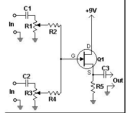
 FET Audio Mixer This simple circuit mixes two or more channels into one channel (eg. stereo into mono). The circuit can mix as many or as few channels as you like and consumes very little power. The mixer is shown with two inputs, but you can add as many as you want by just duplicating the "sections" which are clearly visible on the schematic. R1, R3 2 10K Pot / R2, R4 2 100K 1/4 W Resistor / R5 1 6.8K 1/4 W Resistor C1, C2, C3 3 0.1uF Capacitor / Q1 1 2N3819 Junction FET / MISC 1 Wire, Shielded (Metal) Case, Phono Or Other Plug For Output |
||
  3 Line Mixer 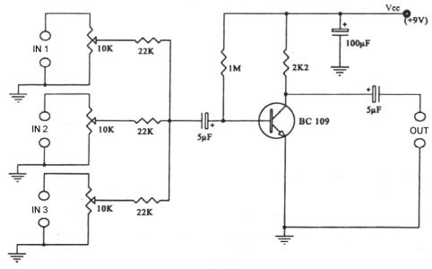 his project is a 3 or more lines mixer. For more than 3 inputs you can repeat the input parts (P=10K R=22K). It powered with 9Vdc. Fm Transmitter    running lights  pwm555  Pulse Width Modulato r 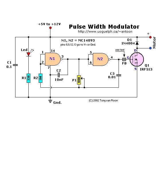 Optimizing the Triacs  A Highly Efficient DC Lamp Dimmer 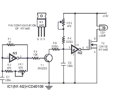 The simplest lamp dimmer cir- cuit consists of a rheostat, in se- ries with the lamp, which one may adjust to obtain the required brightness. Such linear regulators are quite inefficient since a lot of power is wasted in them. Moreover, in the rheostat the moving contacts are likely to get damaged in the long run, as its value is frequently adjusted by moving the slider. Such linear control circuits provide an overall efficiency of no more than 50 per cent. This wastage of power can be avoided if one uses pulse width modulation (PWM) which can be made to control an electronic rheostat. The circuit shown here is based on PWM principle. Gate N1 and its associated components constitute an oscillator producing oscillations of approximately 200 Hz with a pulse width of 0.1 ms. This output is fed to transistor T1 for level shifting. At the output of this transistor is a potentiometer VR2, using which a DC component can be added to the pulses emerging from transistor T1. By adjusting this potentiometer/trimmer, one can have a good linear control of the lamp brightness from completely off state to 100 per cent on state. The signal is inverted by gate N2 and fed to MOSFET 12N10. IC CD40106 provides six inverting buffers with Schmitt trigger action. The buffers are capable of transforming slowly changing input signals into sharply defined jitter-free output signals. They are usually used as wave and pulse shapers. IC CD40106 possesses high immunity and low power consumption of standard CMOS ICs along with the ability to drive 10 LS-TTL loads. In this circuit loads up to 24W can be connected between MOSFET drain and 12V supply without using a heatsink. The loads can even be DC motors, miniature heating elements, etc. If one uses a low RDS (on) MOSFET, a higher efficiency can be achieved. By using the components as shown in the circuit, an efficiency of approximately 95 per cent can be achieved. The flexibility of the design makes it possible to change the MOSFET with a similar one, in case of non-availability of 12N10. The circuit by itself does not draw much current when the load is disconnected. Ensure proper ESD protection while handling the MOSFET to prevent damage. Lab note: The circuit was tested using MOSFET IRF640 with RDS (on)=0.18 ohm. Adjustable Dancing Lights 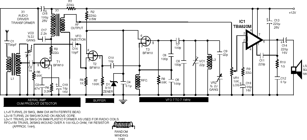 Here is a simple circuit which can be used for decoration purposes or as an indicator. Flashing or dancing speed of LEDs can be adjusted and various dancing patterns of lights can be formed. Audio level meter Christmas Star  Clap Activated Remote 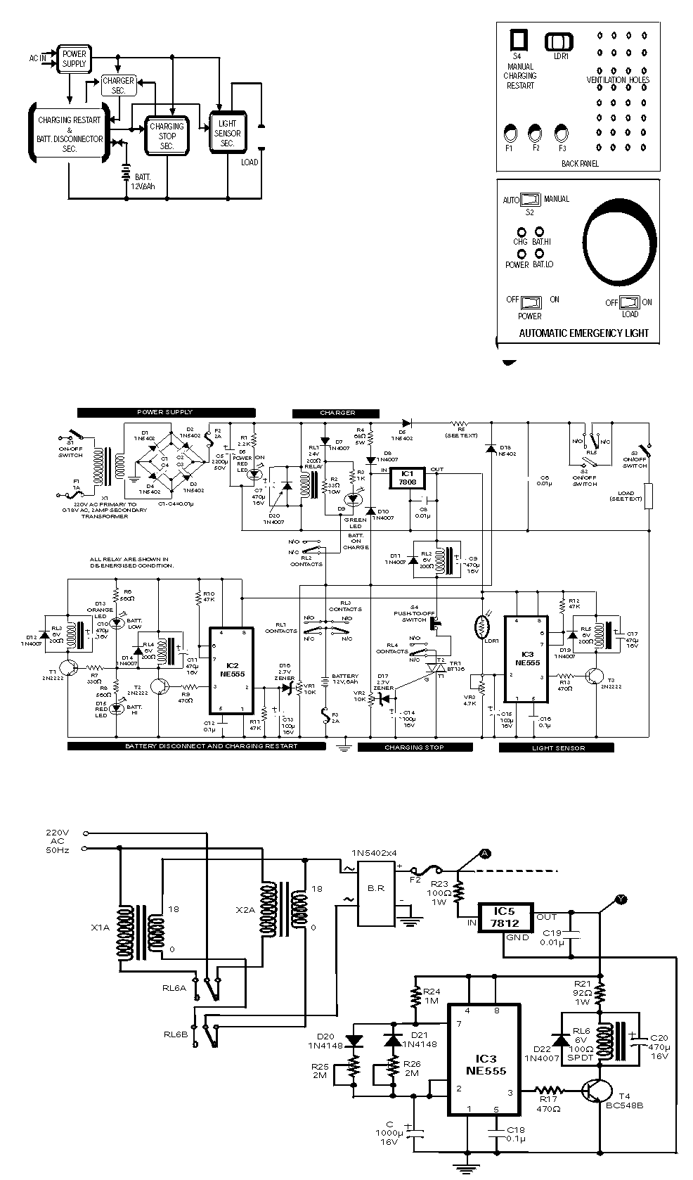 Digital Volume Control 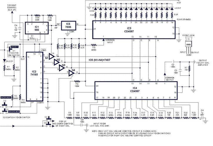 Circuit of a digital volume con- trol using six discrete ICs, in cluding a 5V regulator, is presented. IC1 (555) is configured to function as astable flip-flop. Its frequency or period may be adjusted by proper choice of resistors R44, R45 and capacitor C6 combination. Here it is for 0.3 second period. IC2 is a presetable up/down counter. In this circuit up-mode is used for increasing and down-mode is used for decreasing the volume. IC3 and IC4 are 16-channel analogue multiplexers which function as analogue switches. Here IC3 is used as level indicator while IC4 is used as a potentiometer. Soon after the power is switched on, switch S1 is to be pressed to reset the whole system. When switch S2 is pressed, IC2 counts up the number of pulses and the result is available in the form of BCD output. IC6 is used as an interface between TTL and CMOS ICs. The BCD output controls the address input lines of IC2 and IC3, and selects/switches one, out of sixteen channels, by turning on the appropriate analogue switch. In the circuit, IC4 is used as a potentiometer by connecting 15 resistors (R9 through R23) between each of its 16 input pins and a resistor/capacitor combination of C2, C3 and R7 at its output. The values of resistors R9 through R23 can, of course, be selected as desired. Here the resistors have been selected for a logarithmic scale. Switch S2 is used for increasing and switch S3 is used for decreasing the volume. Similarly, switches S4 and S5 are provided for second channel (right channel) volume control. Also, pin 14 of IC2 can be connected to IC 74193 pin 14 (clear input) of the right channel volume control circuit. The volume control circuit of right channel will be identical to that of the left channel circuit (shown here) except that IC1, IC5 and push-to-on switches are not to be duplicated. A 1µF electrolytic capacitor (C4) is used to prevent switching noise. Resistors R8 and R6 are used to fix the quiescent operating voltage level at half the supply voltage for avoiding distortion of the audio signal from the preamplifier. Capacitors C2, C3 and resistor R7 are provided for proper filtering of the audio and blocking DC component. An exact logarithmic scale of resistors R9 through R23 produces a pleasing and smooth control. Digital Volume Control2  Emergency Light  The circuit of automatic emergency light presented here has the following features: 1. When the mains supply (230V AC) is available, it charges a 12V battery up to 13.5V and then the battery is disconnected from the charging section. 2. When the battery discharges up to 10.2V, it is disconnected from the load and the charging process is resumed. 3. If the mains voltage is available and there is darkness in the room, load (bulb or tube) is turned on by taking power from the mains; otherwise the battery is connected to the load. 4. When the battery discharges up to 10.2V and if the mains is not yet available, the battery is completely disconnected from the circuit to avoid its further discharge. The mains supply of 230V AC is stepped down to 18V AC (RMS) using a 230V AC primary to 0-18V AC, 2A secondary transformer (X1), generally used in 36cm B&W TVs. Diodes D1 through D4 form bridge rectifier and capacitor C5 filters the voltage, providing about 25V DC at the output. Charging section includes 33-ohm, 10-watt resistor R2 which limits the charging current to about 425 mA when battery voltage is about 10.2V, or to 325 mA when battery voltage is about 13.5V. When the battery charges to 13.5V (as set by VR2), zener diode D17 goes into breakdown region, thereby triggering triac TR1. Now, since DC is passing through the triac, it remains continuously ?on? even if the gate current is reduced to zero (by disconnecting the gate terminal). Once the battery is fully charged, charging section is cut-off from the battery due to energisation of relay RL2. This relay remains ?on? even if the power fails because of connection to the battery via diode D10. S4, a normally closed switch, is included to manually restart the charging process if required. Battery disconnect and charging restart section comprises an NE555 timer (IC2) wired in monostable mode. When the battery voltage is above 10.2V (as indicated by red LED D15), zener diode (D16) remains in the breakdown region, making the trigger pin 2 of IC2 high, thereby maintaining output pin 3 in low voltage state. Thus, relay RL3 is ?on? and relay RL4 is ?off.? But as soon as the battery voltage falls to about 10.2V (as set by preset VR1), zener diode D16 comes out of conduction, making pin 2 low and pin 3 high to turn ?on? relay RL4 and orange LED D13. This also switches off relay RL3 and LED D15. Now, if the mains is available, charging restarts due to de-energisation of relay RL2 because when relay RL4 is ?on,? it breaks the circuit of relay RL2 and triac TR1. But if the mains supply is not present, both relays RL3 and RL1 de-energise, disconnecting the battery from the remaining circuit. Thus when battery voltage falls to 10.2 volts, its further discharge is eliminated. But as soon as the mains supply resumes, it energises relay RL1, thereby connecting the battery again to the circuit. Light sensor section also makes use of a 555 timer IC in the monostable mode. As long as normal light is falling on LDR1, its resistance is comparatively low. As a result pin 2 of IC3 is held near Vcc and its output at pin 3 is at low level. In darkness, LDR resistance is very high, which causes pin 2 of IC3 to fall to near ground potential and thus trigger it. As a consequence, output pin 3 goes high during the monostable pulse period, forward biasing transistor T3 which goes into saturation, energising relay RL5. With auto/bypass switch S2 off (in auto mode), the load gets connected to supply via switch S3. If desired, the load may be switched during the day-time by flipping switch S2 to ?on? position (manual). Preset VR3 is the sensitivity control used for setting threshold light level at which the load is to be automatically switched on/off. Capacitors with the relays ensure that there is no chattering of the relays. When the mains is present, diode D8 couples the input voltage to regulator IC1 whereas diode D10 feeds the input voltage to it (from battery) in absense of mains supply. Diode D5 connects the load to the power supply section via resistor R5 when mains is available (diode D18 does not conduct). However, when mains power fails, the situation reverses and diode D18 conducts while diode D5 does not conduct. . The load can be any bulb of 12 volts with a maximum current rating of 2 amperes (24 watts). Resistor R5 is supposed to drop approximately 12 volts when the load current flows through it during mains availability . Hence power dissipated in it would almost be equal to the load power. It is therefore desirable to replace R5 with a bulb of similar voltage and wattage as the load so that during mains availability we have more (double) light than when the load is fed from the battery. For setting presets VR1 and VR2, just take out (desolder one end) diodes D7, D10 and D18. Connect a variable source of power supply in place of battery. Set preset VR1 so that battery-high LED D15 is just off at 10.2V of the variable source. Increase the potential of the variable source and observe the shift from LO BAT LED D13 to D15. Now make the voltage of the source 13.5V and set preset VR2 so that relay RL2 just energises. Then decrease the voltage slowly and observe that relay RL2 does not de-energise above 10.2V. At 10.2V, LED D15 should be off and relay RL2 should de-energise while LED D13 should light up. Preset VR3 can be adjusted during evening hours so that the load is ?on? during the desired light conditions Extension Phone Switcher 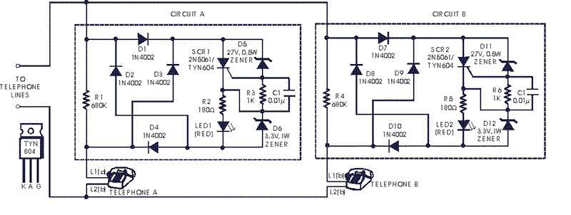 Having multiple extension tele- phones at home is very conve- nient. You can make or receive phone calls practically anywhere in the house. This circuit disables other telephones connected to the phone line whenever a telephone (either the master or any extension phone) is in use. The circuit is inexpensive and is guaranteed to keep the phone conversation private. The circuit does not need an external power supply. It gets its power from the telephone line. The no-load voltage at the telephone line, when the telephone handset is ‘on-hook,’ is around 48 volts. However, when the handset is off-hook, terminal voltage drops to between 5 volts and 15 volts. This is due to the impedance of telephone line and the telephone set. The voltage of the telephone line is the key factor that controls the operation of this circuit. diodes D1, D2, D3 and D4 are connected as bridge rectifier to make the circuit non-polarised. Lifting the handset causes the terminal voltage to drop from 48V to about 10V. The drop in voltage does not, however, occur rapidly. therefore while the terminal voltage is still high (above the threshold voltage level), both zener diodes D5 and D6 are turned on. Current flows through resistor R3, triggering SCR1 and providing a link to the telephone set connected to lines L1(a) and L2(a). When the terminal voltage drops below the threshold voltage of the zener diode, diode D5 reverts to its non-conducting state, cutting off the gate drive to SCR1. However, once the SCR is on, it will remain in that state as long as the current flowing through it does not fall to near zero level. Thus the link continues. Zener D6 maintains the voltage across resistor R2 and LED1/LED2 indicates as to which telephone is in use. The low off-hook voltage of the line will disable the other extension phones. The line voltage will not turn on zener diodes D11 and D12, even if the handsets of the other extension phones are lifted. Use the following procedure to check up the system after wiring: Four-in-one burglar alarm 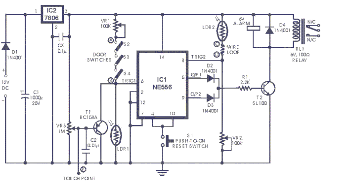 In this circuit, the alarm will be switched on under the following four different conditions: 1. When light falls on LDR1 (at the entry to the premises). 2. When light falling on LDR2 is obstructed. 3. When door switches are opened or a wire is broken. 4. When a handle is touched. The light dependent resistor LDR1 should be placed in darkness near the door lock or handle etc. If an intruder flashes his torch, its light will fall on LDR1, reducing the voltage drop across it and so also the voltage applied to trigger 1 (pin 6) of IC1. Thus transistor T2 will get forward biased and relay RL1 energise and operate the alarm. Sensitivity of LDR1 can be adjusted by varying preset VR1. LDR2 may be placed on one side of a corridor such that the beam of light from a light source always falls on it. When an intruder passes through the corridor, his shadow falls on LDR2. As a result voltage drop across LDR2 increases and pin 8 of IC1 goes low while output pin 9 of IC1 goes high. Transistor T2 gets switched on and the relay operates to set the alarm. The sensitivity of LDR2 can be adjusted by varying potentiometer VR2. A long but very thin wire may be connected between the points A and B or C and D across a window or a door. This long wire may even be used to lock or tie something. If anyone cuts or breaks this wire, the alarm will be switched on as pin 8 or 6 will go low. In place of the wire between points A and B or C and D door switches can be connected. These switches should be fixed on the door in such a way that when the door is closed the switch gets closed and when the door is open the switch remains open. If the switches or wire, are not used between these points, the points should be shorted. With the help of a wire, connect the touch point (P) with the handle of a door or some other suitable object made of conducting material. When one touches this handle or the other connected object, pin 6 of IC1 goes ‘low’. So the alarm and the relay gets switched on. Remember that the object connected to this touch point should be well insulated from ground. For good touch action, potentiometer VR3 should be properly adjusted. If potentiometer VR3 tapping is held more towards ground, the alarm will get switched on even without touching. In such a situation, the tapping should be raised. But the tapping point should not be raised too much as the touch action would then vanish. When you vary potentiometer VR1, re-adjust the sensitivity of the touch point with the help of potentiometer VR3 properly. If the alarm has a voltage rating of other than 6V (more than 6V), or if it draws a high current (more than 150 mA), connect it through the relay points as shown by the dotted lines. As a burglar alarm, battery backup is necessary for this circuit. Note: Electric sparking in the vicinity of this circuit may cause false triggering of the circuit. To avoid this adjust potentiometer VR3 properly. Handy Telephone Receiver 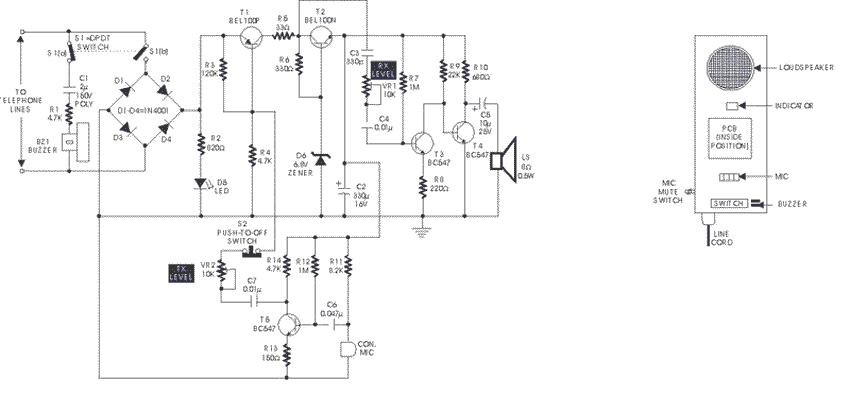 An interesting circuit for a me- dium performance handy elec- tronic telephone receiver, suited for receiving incoming calls, is described here. This circuit can be connected to almost all types of telephone exchange lines. To simplify the gadget, the dialler section has been omitted. The circuit can be constructed on a medium size veroboard. Wiring and components layout are not very critical. For compactness, enclose the wired circuit in a plastic cabinet as shown in Fig.(a) here. In order to prevent undesired acoustic feedback, it is necessary to adjust the orientation of ear-piece (LS) and mouth-piece (MIC) at the final stage of construction. The circuit consists of four sections: ringer, voltage regulator, transmitter and receiver. The ringer section is built around capacitor C1, resistor R1 and electronic buzzer BZ1. No readymade ringer ICs are used here, deliberately, to minimise the space. Transistor T1 is the main interface transistor. Transistor T2, in conjuction with resistor R6 and zener diode D6, works as a constant voltage regulator which provides an output of 6V DC. This supply is used to bias the remaining circuit. Capacitor C2 is used as the filter capacitor. Receiver section is wired around transistors T3 and T4 which form a high-gain direct coupled amplifier. Voice input from the collector of transistor T1 is connected to the base of transistor T3 via capacitor C3 and preset VR1 and capacitor C4. Preset VR1 is for receiver level adjustment. A small loudspeaker is used as the ear-piece. Circuit comprising transistor T5, condenser mic and associated components functions as the transmitter circuit. Output signals from this section are applied to the base of transistor T1 via capacitor C7 and preset VR2. Preset VR2 is for transmit level control. Microphone muting is provided by push-to-off switch S2. Initially, set the presets VR1 and VR2 in their respective mechanical middle positions and readjust both to get the best performance using trial and error method. IR Remote Control  Here is a circuit which can switch on and switch off any appliance with the help of a common type of infra-red remote control (transmitter). This circuit senses the IR pulse and then controls the appliance accordingly. The circuit functions such that a short pulse from the remote tran- smitter switches on the triac (and the load) while a longer pulse switches off the triac as also the load. The circuit is built around hex inverter IC CD 4049. When the infra-red pulse is received by the sensor, its output (Note: Here VR1 denotes the in-circuit resistance of preset VR1.) The output of multivibrator is fed to the base of current amplifier 2N3055 via resistor R2 (1kilo-ohm). The brakelight bulb is connected in series with the collector of 2N3055. The flashing rate of this bulb is adjusted by 100k preset (VR1). Transistor 2N3055 may get heated due to high current switching action; hence a small heatsink, similar to the type used in television power supply, is recommended. The category of 2-wheelers which do not have a battery, can use the bridge rectifier circuit shown here. Several designs of round, square and rectangular reflectors are available which may be used in conjunction with any suitable 12V bulb with proper rating (around 20 watts). However, if flashing of the brake- light affects intensity of headlight bulb, reduce the rating of brakelight bulb to 10 watts. Off-Line Telephone Tester 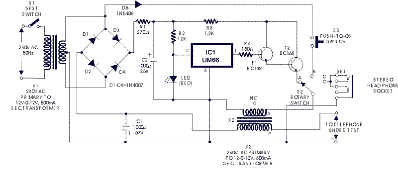 Here is a circuit of an off-line telephone tester which does not require any telephone line for testing a telephone instrument. The circuit is so simple that it can be easily assembled even by a novice having very little knowledge of electronics. A telephone line may be considered to be a source of some 50 volts DC with a source impedance of about 1 kilo-ohm. During ringing, in place of DC, an AC voltage of 70 to 80 volts (at 17 to 25 Hz) is present across the telephone line. When the subscriber lifts the handset, the same is sensed by the telephone exchange and the ringing AC voltage is disconnected and DC is reconnected to the line. Lifting of the handset from the telephone cradle results in shunting of the line’s two wires by low impedance of the telephone instrument. As a result, 50V DC level drops to about 12 volts across the telephone instrument. During conversation, the audio gets superimposed on this DC voltage. Since any DC supply can be used for testing a telephone instrument, the same is derived here from AC mains using step-down transformer X1. Middle point of the transformer’s secondary has been used as common for the two full-wave rectifiers—one comprising diodes D1 and D2 together with smoothing capacitor C1 and the other formed by diodes D3 and D4 along with filter capacitor C2. The former supplies about 12 volts for the telephone instrument through primary of transformer X2 which thus simulates a source impedance, and a choke which blocks AC audio signals present in the secondary of transformer X2. The AF signal available in secondary of X2 is sufficiently strong to directly drive a 32-ohm headset which is connected to the circuit through headphone socket SK1 via rotary switch S2. During ringing, a pulsating DC voltage from transformer X1 via rectifier diode D5, push-to-on switch S3, and contact ‘B’ of rotary switch S2 is applied across secondary of transformer X2. The boosted voltage available across primary of transformer X2 is sufficient to drive the ringer in the telephone instrument. Please avoid pressing of switch S3 for more than a few seconds at a time to prevent damage to the circuit due to high voltage across primary of transformer X2. The circuit also incorporates a music IC (UM66) whose output is connected to secondary of transformer X2 via switch S2 after suitably boosting its output with the help of darlington transistor pair T1 and T2. This output can be used to test the audio section of any telephone instrument. After having assembled the circuit satisfactorily, the following procedure may be followed for testing a telephone instrument: Programmable Musical Bell 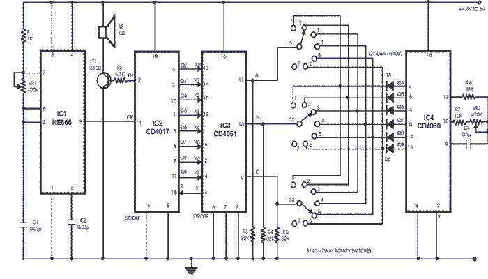 The circuit presented here is that of a musical bell which may be programmed for generation of a number of musical notes. The complete working of the circuit is explained below. IC1 timer (NE555) is wired as an astable multivibrator operating in audio band. Frequency of the timer IC may be varied with the help of potmeter VR1. The output of IC1 at the selected frequency of operation is coupled to the clock input of IC2 (CD4017). IC2 divides the input frequency by an integer ‘n’. The value of ‘n’ depends on its output pin number which is connected to its own reset pin 15. In this circuit the maximum value of ‘n’ that may be selected is 8. This selection is carried out with the help of CD4051 (IC3) which is a CMOS 8-input analogue multiplexer whose function here is to make an electrical connection between specified output of IC2 and pin 15 of IC2 . The output of IC2, which is connected to its pin 15, depends on the binary number present at the address input pins 9 through 11 of IC3 CD4051. Thus by changing the binary number applied to the address control input of IC3, the value of ‘n’ as also the frequency division ratio can be changed. The final output Q1 after frequency division available at pin 2 of IC2 is amplified by transistor T1(SL100). Different frequency division ratios produce different tones from the speaker. The different tones are connected serially in a particular sequence to produce various musical notes. This is achieved through IC4 (CD4060) which is a 14-bit binary counter. Delay time of tone is adjusted with the help of potmeter VR2. Changing the arrangement of tones in the sequence (and also the delay introduced in each tone) will result into different musical notes. Switches S1, S2 and S3 serve this purpose. Try different positions of switches S1, S2 and S3 and delay control potmeter VR2 to abtain different notes into the speaker. Use potmeter VR1 to change the tone. Rain Alarm 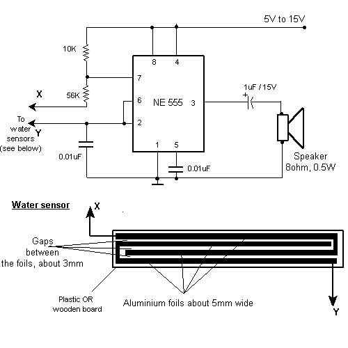 Ready-to-use Object Counter 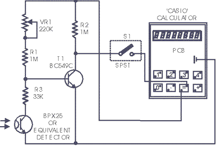 Presented here is the cheapest 8-digit programmable object or event counter. It is a fail-proof, fool-proof, power failure-proof, one evening project. A general-purpose (arithmetic) calculator has some inherent shortcomings which can, however, be used in many ways by proper programming sequences. For example, there is no squaring key in a general-purpose calculator, but it can not only square it has even the inherent capability of a single touch successive multiplication, thus giving us a choice of making a geometric progression (G.P.) or successive addition or forming an arithmetic progression (A.P.). For example, operating the keys 5,x,=,=,... you obtain the G.P. 5,25,125,625,... or by operating keys 5,x,4,=,=,=,..., you get the G.P.: 4,20, 100,500,... Next, operate keys: 5,+, 2,=,=,... to get the A.P.: 5,7,9,11,13,... The latter facility (A.P.) has been used here to count the objects by programming the calculator keys 1,+,=,=,... When you open the calculator (such as ‘Casio’), you will find that the conductive silicon key pads bridge the two terminals of a key, when depressed. Locate the switch terminals for (=) key and check the polarity of the terminals with respect to the battery negative. The terminal which is found to be positive is to be connected to the junction of R2 and VR1, and the other terminal is to be connected to switch S1 as shown in the figure. The negative battery terminal is to be connected to emitters of photo-transistor and transistor T1. (There may be slight difference in the use of key terminals in different brands of calculators.) The optical sensor used here is BPX25, a very sensitive photo-transistor which has a built-in lens to focus the incident light on to the chip. Only two leads, emitter and collector, have been used. When light falls on the sensor, it conducts as if it had got forward biased. A variable resistor of 220k in series with another fixed resistor of 1 M (selected by trial) has been used at the base of transistor T1 (BC149C/BC 549C) to set the threshold level for its conduction, depending upon the intensity of light used. When light is obstructed, BPX goes to cut-off, transistor T1 conducts and the terminal of (=) key which is connected via switch S1 (assuming closed), goes low. This is equivalent to depression of the (=) key. When light again falls on the sensor, it conducts and the base of transistor T1 goes low, throwing it to cut-off, so that its collector and hence the (=) key gets connected to the positive bus via 1 M resistor R2. A pulse is passed on and the calculator advances by 1. Current drain from the battery is less than 50 µA, which a button cell can easily provide. The counter is slow but there is no switch debouncing effect present, which makes the counter highly reliable and ideal as a slow event counter in applications such as visitor counter. Further, the circuit is auto-locked, since any resetting is possible only when BPX is in the cut-off position, i.e., in darkness. To program, cover the phototran- sistor and operate keys : 1,+,=. In case of a deadlock in programming, miniature switch S1 may be used to enable isolation of the (=) key. Set the 220k preset according to the ambient and the incident light, so that the calculator counts when light is cut-off and again allowed to fall when obstruction is removed. If it is used to count visitors in a well day-lighted environment, only a white washed wall or a white paper pasted on the opposite door panel is sufficient. For indoor applications, a specific source of light is required. Both the source of light as well as the BPX should then be mounted in opaque (preferably black) tubes and a lens be fitted in the light-source tube to focus the light on to the photo-transistor. BC149C/549C is preferred due to its large current gain of the order of 300 at 10 µA, compared to 150 that of BC548B, so that the instrument becomes more sensitive. Running Lights Effect 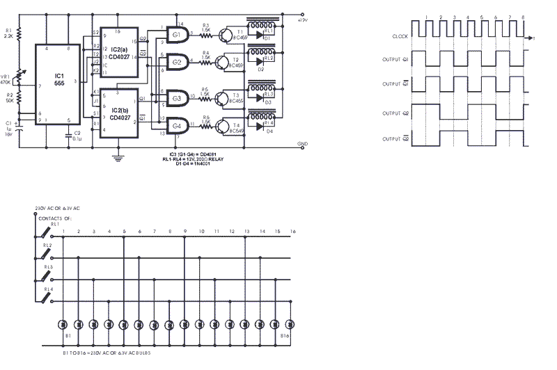 This is a simple but novel idea for achieving ‘running lights effect’. It is quite different from the electrical drum and contact system used for decorating buildings etc. It can be used commercially for attaining desired visual effects. Tank Overflow Preventer 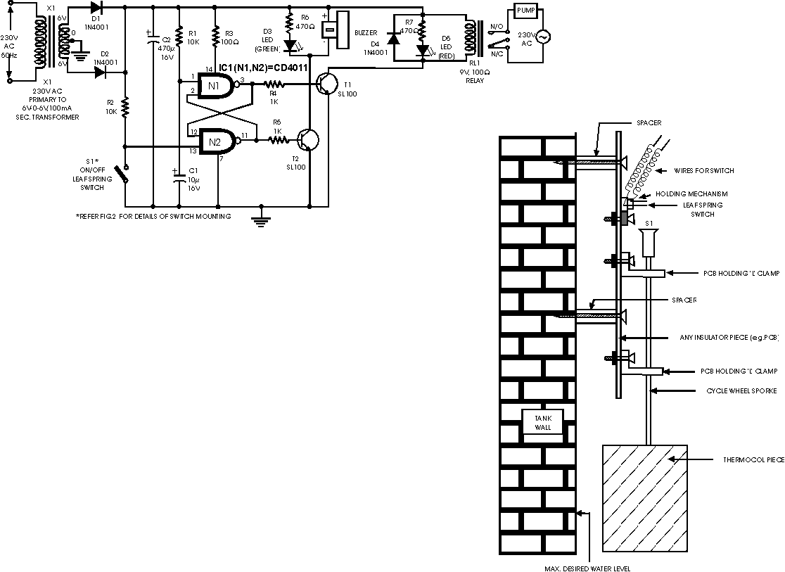 There is practically no house without an overhead tank (OHT). People who use electrically-operated water pumps for filling the OHT find it very inconvenient to switch off the pump when their overhead tank starts overflowing, specially when they are busy. So there is plenty of water wastage as well as wastage of power (consumed by the pump). However, there is a solution to get rid of this headache. The circuit given here will switch off the pump and also generate a melodious tune when the overhead tank gets filled up to the maximum desired level. All you have to do is switch off the power supply to the circuit when you are relatively free. The heart of the circuit is the CMOS latch CD4001. Usually the latch can be operated in two modes, namely, set and reset mode, i.e. the latch output can be set to logic 1 or reset to logic 0 by applying appropriate active low level input signal to pins 1 and 13, respectively. Here, in the given circuit, the set point is pin 1 and the reset point is pin 13. The inverted output of the latches are obtained at pins 3 and 11, respectively. When the circuit is powered there is a voltage drop at pin 1 due to the resistor-capacitor R1-C1 combination. The values of resistor R1 and C1 are chosen in such a way that pin 1 is low for about two seconds which is sufficient to energise the relay through transistor T1 and thus the pump starts running. When sufficient water gets filled in the overhead tank, switch S1 in the sensing unit, in the overhead tank as shown in Fig. 2, sends an active low signal to pin 13 which resets latch gate N1 output to logic 0. This causes transistor T1 to stop conducting, thereby de-energising the relay and shutting down the pump. At the same time, the output at pin 11 of gate N2 will be logic 1. This results in conduction of transistor T2 and melodious buzzer sounds. The green LED also lights up while the red LED, which remains on as long as the relay remains energised, gets switched off when water reaches the specified level in the overhead tank. The circuit possesses the following advantages: Telephone Call Counter 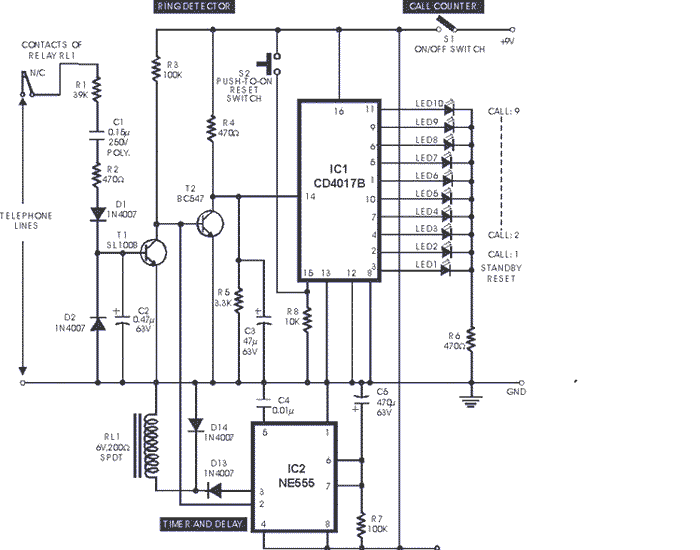 The circuit presented here is a very useful add-on device to be connected to the telephone lines to count and display the number of incoming calls received in the absence of the subscriber. The circuit can be fabricated using low-cost and easily available components. It uses a popular decade counter IC, a timer IC, and a few other discrete components. The circuit may be divided into three sections: (a) ring detector, (b) call counter, and (c) timer and relay controller. The ring detector circuit detects the incoming ring signals. The timer circuit is used to control a relay, which controls the switching of ring signals to the ring detector section. The call counter is used to count the number of incoming calls. To count the number of calls (not the number of rings), the response of the counter is limited to the first ring pulse only. In other words, it responds to the initial ring pulse and ignores subsequent ring pulses which repeat till the calling subscriber or the telephone exchange cuts them off. When power switch S1 is turned on, the circuit gets 9V supply from the battery and the reset indicator LED1 lights up. If LED1 does not glow initially, press S2 until it glows. Now, in this standby mode, transistor T1 is in nonconducting state. But transistor T2 is forward biased via resistor R3. As a result pin 14 of IC1 is at a low potential. When the telephone rings, ac voltage of about 75 volts appears across the input terminals of the circuit. During positive half cycles of the ring signal, D1 starts conducting and transistor T1 gets forward biased. When transistor T1 conducts, transistor T2 gets reverse biased. Consequently, pin 14 of IC1 gets a short positive pulse through R4 and LED2 starts glowing, indicating call number 1. Simultaneously IC2 (which is wired as a monostable flip-flop) is triggered by the ring detector circuit and the relay gets energised. As a result the circuit is disconnected from the telephone lines for a predetermined period (decided by resistor R7 and capacitor C5 values). At the end of the mono time period, the circuit automatically returns to monitor the telephone line for the next call. This operation cycle is repeated with each succeeding call. This circuit is capable of indicating up to 9 calls which are received in the absence of subscriber. It can be extended for more calls by cascading the required number of CD4017B ICs. UltraSonic Switch 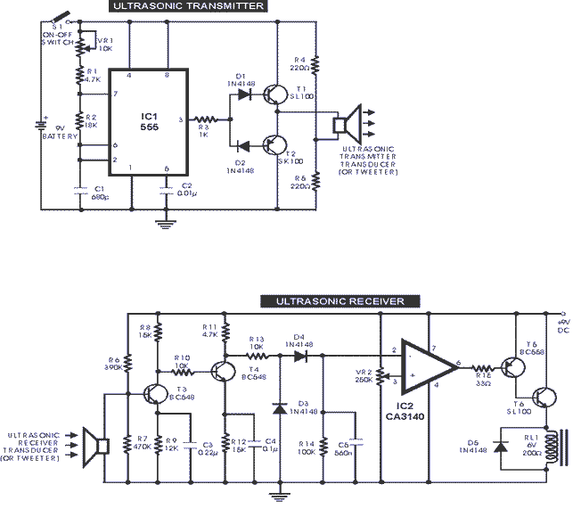 Circuit of a new type of remote control switch is described here. This circuit functions with inaudible (ultrasonic) sound. Sound of frequency up to 20 kHz is audible to human beings. The sound of frequency above 20 kHz is called ultrasonic sound. The circuit described generates (transmits) ultrasonic sound of frequency between 40 and 50 kHz. As with any other remote control system this cirucit too comprises a mini transmitter and a receiver circuit. Transmitter generates ultrasonic sound and the receiver senses ultrasonic sound from the transmitter and switches on a relay. The ultrasonic transmitter uses a 555 based astable multivibrator. It oscillates at a frequency of 40-50 kHz. An ultrasonic transmitter transducer is used here to transmit ultrasonic sound very effectively. The transmitter is powered from a 9-volt PP3 single cell. The ultrasonic receiver circuit uses an ultrasonic receiver transducer to sense ultrasonic signals. It also uses a two-stage amplifier, a rectifier stage, and an operational amplifier in inverting mode. Output of op-amp is connected to a relay through a complimentary relay driver stage. A 9-volt battery eliminator can be used for receiver circuit, if required. When switch S1 of transmitter is pressed, it generates ultrasonic sound. The sound is received by ultrasonic receiver transducer. It converts it to electrical variations of the same frequency. These signals are amplified by transistors T3 and T4. The amplified signals are then rectified and filtered. The filtered DC voltage is given to inverting pin of op-amp IC2. The non- inverting pin of IC2 is connected to a variable DC voltage via preset VR2 which determines the threshold value of ultrasonic signal received by receiver for operation of relay RL1. The inverted output of IC2 is used to bias transistor T5. When transistor T5 conducts, it supplies base bias to transistor T6. When transistor T6 conducts, it actuates the relay. The relay can be used to control any electrical or electronic equipment. Important hints: Water Level Controller Using 3-Phase Starter 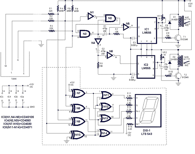 Generally overhead tanks are filled with water by operating a 3-phase pump in conjunction with starter, manually. You have no control over the level to which it may be filled. It may cause overflow or water level may remain too low when you switch off the pump motor. Manual operation of the motor pump starter is thus not advisable. Present circuit may be added to the existing manual 3-phase starter of the pump motor so that it may be operated automatically as well as manually. Four sensor probes made up of brass or stainless steel stiff wires or rods may be hung firmly in the tank. Probes marked E and L are hung with their bottoms near the bottom level of the tank at which we wish to start the pump. The probe H is hung with its bottom at a level at which we wish to stop the pump. Probe M is hung with its bottom end in between those of probes E and H. It is used for indication (only) of middle level. Sensors M, L, and H are connected with resistors R1, R2, and R3, whereas probe E is directly connected to ground. Resistors R1, R2, and R3 are connected to 12V supply through resistors R4, R5, and R6, respectively. The connections of various ICs, gates and other components are shown in the figure. The N/C contacts of relay RL1 are conne- cted in series with the ‘off’ push button of 3-phase st- arter of pump mo- tor. The N/O contact of relay RL2 is connected in parallel to the ‘on’ push button of the 3-phase starter. Circuit shown within the dotted lines is the optional circuit of the water level indicator. When the wa- ter level in the ta- nk is below pro- bes E and L, output of gate N1 is logic low and ou- tput of gate N2 is latched to logic high level. Simu- ltaneously output of gate N3 goes logic low and is inverted by inverter N4. This is differentiated by R-C network for- med using resistor R8 and capacitor C2, and the resulting po- sitive going pulse inverted by inv- erter N6 is given to trigger pin of timer IC2. IC2 is wired as a monostable flip-flop. The output positive going pulse appearing at pin 3 energises relay RL2 for short duration to operate the 3-phase starter for the pump motor. As the water starts filling in the tank and ultimately touches probe H, the output of gate N3 goes high. This is differentiated by resistor R7 and capacitor C1. The positive going pulse appearing at resistor R7 is inverted by gate N5 and applied to trigger pin of monostable flip-flop IC1. The output of IC1 is used to energise relay RL1 via driver transistor T1. This results in opening of N/C contact in series with the stop button of starter and thus switching off of the pump motor. Water level status is displayed using IC5 and IC6 in conjunction with 7-segment display DIS-1. The display indicates F for full, H for half, L for low level, and E for empty condition. It may be noted that probes E and L must be fitted at a level slightly higher than the exit (vent) plug of the tank. DC- DC Converter 12V to 24V  This simple circuit is a DC-DC converter that converting up 12V source to a 24V. It can be used to run radios, small lights, relays, horns and other 24V accessories from a 12V vehicle with a maximum draw of about 800mA. This DC-DC Converter can be used to charge one 12V battery from another, or step up the voltage just enough to provide necessary overhead for a 12V linear regulator. Using one op-amp as a squarewave oscillator to ring an inductor and another op-amp in a feedback loop, it won't... Low Cost Universal Battery Charger  Here is the circuit diagram of a low cost universal charger for NiCD - NiMH batteries. This circuit is Ideal for car use. It has ability to transform a mains adapter in to a charger . This one can be used to charge cellular phone, toys, portables, video batteries, MP3 players, ... and has selectable charge current. An LED is located in circuit to indicate charging. Can be built on a general purpose PCB or a veroboard. I hope you really like it. LED function indication. Two Flashing LEDs Circuit 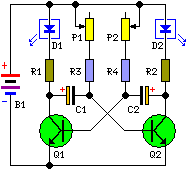 Here is the circuit diagram of Two Flashing LED's for different applications (such as model construction), and recreational. Having adjustable flashing speed with two potentiometers. It is the collection of a few active and passive components. This circuit is very easy to built ( a good idea for beginners ) and can be build on a general purpose pcb or on a veroboard. The complete picture and schematic of this project is shown below |
||